 | –≠–Ľ–Ķ–ļ—ā—Ä–ĺ–Ĺ–Ĺ—č–Ļ –ļ–ĺ–ľ–Ņ–ĺ–Ĺ–Ķ–Ĺ—ā: MAT04FY | –°–ļ–į—á–į—ā—Ć:  PDF PDF  ZIP ZIP |
ńÓÍůžŚŪÚŗŲŤˇ Ť ÓÔŤŮŗŪŤˇ www.docs.chipfind.ru
REV. D
Information furnished by Analog Devices is believed to be accurate and
reliable. However, no responsibility is assumed by Analog Devices for its
use, nor for any infringements of patents or other rights of third parties that
may result from its use. No license is granted by implication or otherwise
under any patent or patent rights of Analog Devices.
a
MAT04
Matched Monolithic
Quad Transistor
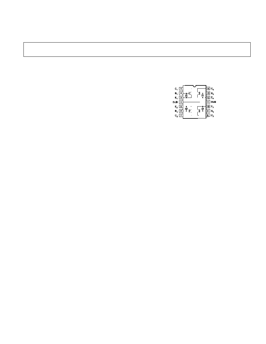
PIN CONNECTIONS
14-Lead Cerdip (Y Suffix)
14-Lead Plastic DIP (P Suffix)
14-Lead SO (S Suffix)
FEATURES
Low Offset Voltage: 200 V max
High Current Gain: 400 min
Excellent Current Gain Match: 2% max
Low Noise Voltage at 100 Hz, 1 mA: 2.5 nV/
Hz max
Excellent Log Conformance: rBE = 0.6 max
Matching Guaranteed for All Transistors
Available in Die Form
PRODUCT DESCRIPTION
The MAT04 is a quad monolithic NPN transistor that offers ex-
cellent parametric matching for precision amplifier and nonlin-
ear circuit applications. Performance characteristics of the
MAT04 include high gain (400 minimum) over a wide range of
collector current, low noise (2.5 nV/
Hz maximum at 100 Hz,
I
C
= 1 mA) and excellent logarithmic conformance. The
MAT04 also features a low offset voltage of 200
ĶV and tight
current gain matching, to within 2%. Each transistor of the
MAT04 is individually tested to data sheet specifications. For
matching parameters (offset voltage, input offset current, and
gain match), each of the dual transistor combinations are
verified to meet stated limits. Device performance is guaranteed
at 25
įC and over the industrial and military temperature ranges.
The long-term stability of matching parameters is guaranteed by
the protection diodes across the base-emitter junction of each
transistor. These diodes prevent degradation of beta and match-
ing characteristics due to reverse bias base-emitter current.
The superior logarithmic conformance and accurate matching
characteristics of the MAT04 makes it an excellent choice for
use in log and antilog circuits. The MAT04 is an ideal choice in
applications where low noise and high gain are required.
One Technology Way, P.O. Box 9106, Norwood, MA 02062-9106, U.S.A.
Tel: 781/329-4700
www.analog.com
Fax: 781/326-8703
© Analog Devices, Inc., 2002
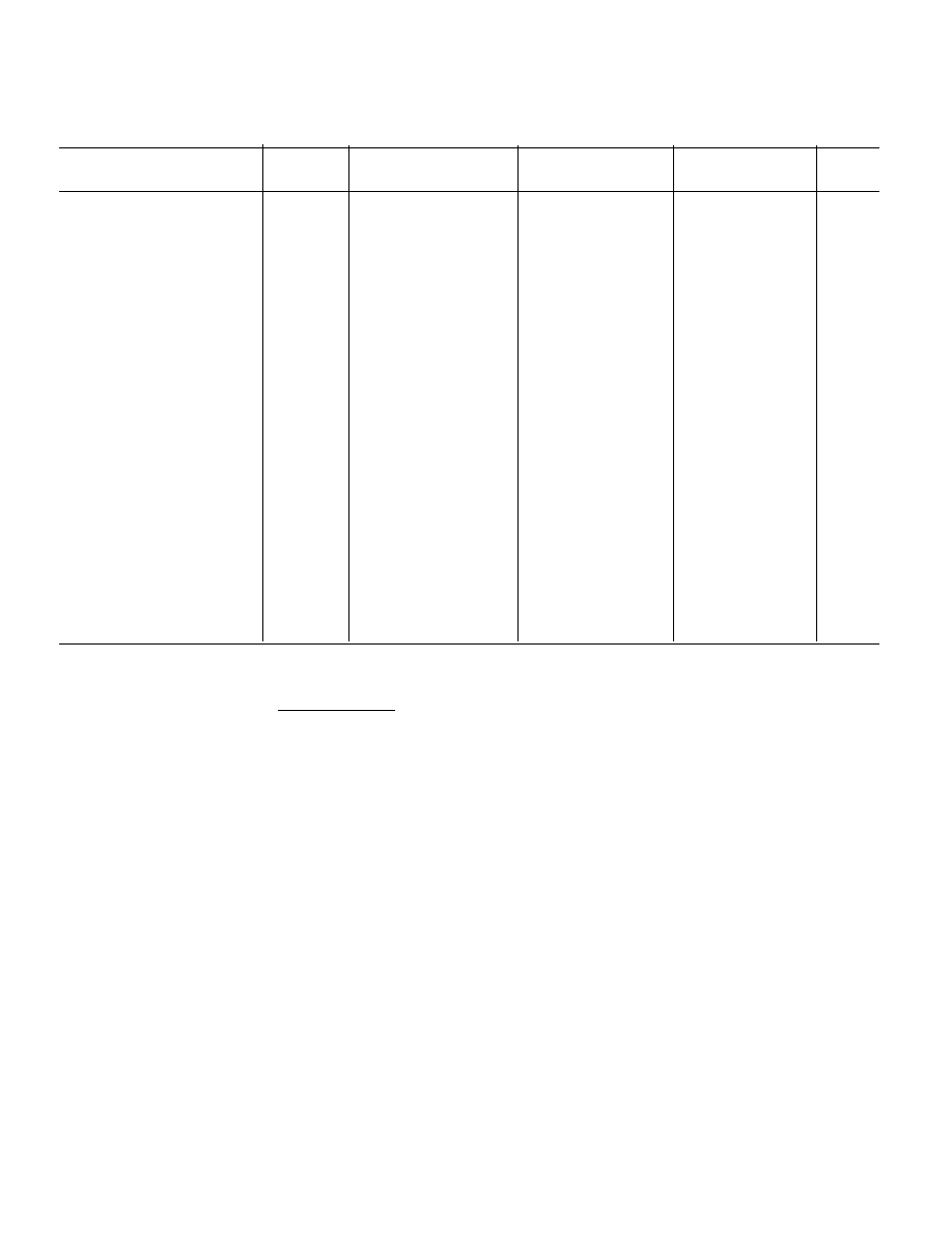
ELECTRICAL CHARACTERISTICS
(@ T
A
= 25 C unless otherwise noted. Each transistor is individually tested. For matching
parameters (V
OS
, I
OS
,
h
FE
) each dual transistor combination is verified to meet stated limits. All tests made at endpoints unless otherwise noted.)
MAT04E
MAT04F
Parameter
Symbol
Conditions
Min
Typ
Max
Min
Typ
Max
Unit
Current Gain
h
FE
10
ĶA I
C
1 mA
0 V
V
CB
30 V
1
400
800
300
600
Current Gain Match
h
FE
I
C
= 100
ĶA
0 V
V
CB
30 V
2
0.5
2
1
4
%
Offset Voltage
V
OS
10
ĶA I
C
1 mA
0 V
V
CB
30 V
3
50
200
100
400
ĶV
Offset Voltage Change vs.
V
OS
/
I
C
10
ĶA I
C
1 mA
Collector Current
V
CB
= 0 V
3
5
25
10
50
ĶV
Offset Voltage Change vs. V
CB
V
OS
/
V
CB
10
ĶA I
C
1 mA
0 V
V
CB
30 V
3
50
100
100
200
ĶV
Bulk Emitter Resistance
r
BE
10
ĶA I
C
1 mA
V
CB
= 0 V
4
0.4
0.6
0.4
0.6
Input Bias Current
I
B
I
C
= 100
ĶA
0 V
V
CB
30 V
125
250
165
330
nA
Input Offset Current
I
OS
I
C
= 100
ĶA; V
CB
= 0 V
0.6
5
2
13
nA
Breakdown Voltage
BV
CEO
I
C
= 10
ĶA
40
40
V
Collector Saturation Voltage
V
CE(SAT)
I
B
= 100
ĶA; I
C
= 1 mA
0.03
0.06
0.03
0.06
V
Collector-Base Leakage Current
I
CBO
V
CB
= 40 V
5
5
pA
Noise Voltage Density
e
n
V
CB
= 0 V; f
O
= 10 Hz
2
3
2
4
nV/
Hz
I
C
= 1 mA; f
O
= 100 Hz
1.8
2.5
1.8
3
nV/
Hz
f
O
= 1 kHz
5
1.8
2.5
1.8
3
nV/
Hz
Gain Bandwidth Product
f
T
I
C
= 1 mA; V
CE
= 10 V
300
300
MHz
Output Capacitance
C
OBO
V
CB
= 15 V; I
E
= 0
f = 1 MHz
10
10
pF
Input Capacitance
C
EBO
V
BE
= 0 V; I
C
= 0
f = 1 MHz
40
40
pF
NOTES
1
Current gain measured at I
C
= 10
ĶA, 100 ĶA and 1 mA.
2
Current gain match is defined as:
h
I
h
I
FE
B
FE
MIN
C
=
100(
)(
)
3
Measured at I
C
= 10
ĶA and guaranteed by design over the specified range of I
C
.
4
Guaranteed by design.
5
Sample tested.
Specifications subject to change without notice.
≠2≠
REV. D
MAT04≠SPECIFICATIONS
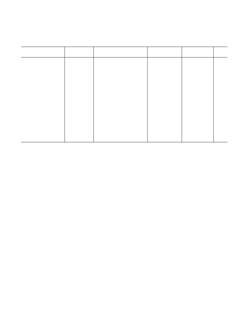
ELECTRICAL CHARACTERISTICS
(at ≠25 C
T
A
85 C for MAT04E, ≠40 C
T
A
85 C for MAT04F, unless
otherwise noted. Each transistor is individually tested. For matching parameters (V
OS
, I
OS
) each dual transistor combination is
verified to meet stated limits. All tests made at endpoints unless otherwise noted.)
MAT04E
MAT04F
Parameter
Symbol
Conditions
Min
Typ
Max
Min
Typ
Max
Unit
Current Gain
h
FE
10
ĶA I
C
1 mA
0 V
V
CB
30 V
1
225
625
200
500
Offset Voltage
V
OS
10
ĶA I
C
1 mA
0 V
V
CB
30 V
2
60
260
120
520
ĶV
Average Offset
TCV
OS
I
C
= 100
ĶA
Voltage Drift
V
CB
= 0 V
3
0.2
1
0.4
2
ĶV/įC
Input Bias Current
I
B
I
C
= 100
ĶA
0 V
V
CB
30 V
160
445
200
500
nA
Input Offset Current
I
OS
I
C
= 100
ĶA
V
CB
= 0 V
4
20
8
40
nA
Average Offset
TCI
OS
I
C
= 100
ĶA
Current Drift
V
CB
= 0 V
50
100
pA/
įC
Breakdown Voltage
BV
CEO
I
C
= 10
ĶA
40
40
V
Collector-Base
I
CBO
V
CB
= 40 V
Leakage Current
0.5
0.5
nA
Collector-Emitter
I
CES
V
CE
= 40 V
Leakage Current
5
5
nA
Collector-Substrate
I
CS
V
CS
= 40 V
Leakage Current
0.7
0.7
nA
MAT04
≠3≠
REV. D
REV. D
MAT04
≠4≠
ABSOLUTE MAXIMUM RATINGS
1
Collector-Base Voltage (BV
CBO
) . . . . . . . . . . . . . . . . . . . 40 V
Collector-Emitter Voltage (BV
CEO
) . . . . . . . . . . . . . . . . . 40 V
Collector-Collector Voltage (BV
CC
) . . . . . . . . . . . . . . . . . 40 V
Emitter-Emitter Voltage (BV
EE
) . . . . . . . . . . . . . . . . . . . 40 V
Collector Current . . . . . . . . . . . . . . . . . . . . . . . . . . . . . 30 mA
Emitter Current . . . . . . . . . . . . . . . . . . . . . . . . . . . . . . . 30 mA
Substrate (Pin-4 to Pin-11) Current . . . . . . . . . . . . . . . 30 mA
Operating Temperature Range
MAT04EY . . . . . . . . . . . . . . . . . . . . . . . . . ≠25
įC to +85įC
MAT04FY, FP, FS . . . . . . . . . . . . . . . . . . . ≠40
įC to +85įC
Storage Temperature
Y Package . . . . . . . . . . . . . . . . . . . . . . . . . ≠65
įC to +150įC
P Package . . . . . . . . . . . . . . . . . . . . . . . . . ≠65
įC to +125įC
Lead Temperature (Soldering, 60 sec) . . . . . . . . . . . . +300
įC
Package Type
JA
2
JC
Units
14-Lead Cerdip
108
16
įC/W
14-Lead Plastic DIP
83
39
įC/W
14-Lead SO
120
36
įC/W
NOTES
1
Absolute maximum ratings apply to both DICE and packaged parts, unless
otherwise noted.
2
JA
is specified for worst case mounting conditions, i.e.,
JA
is specified for
device in socket for cerdip and P-DIP packages;
JA
is specified for device
soldered to printed circuit board for SO package.
ORDERING GUIDE
T
A
= 25 C
Temperature
Package
Package
Model
V
OS
max
Range
Description
Option
MAT04EY
*
200
ĶV
≠25
įC to +85įC
Cerdip
Q-14
MAT04FY
*
400
ĶV
≠40
įC to +85įC
Cerdip
Q-14
MAT04FP
400
ĶV
≠40
įC to +85įC
P-DIP-14
N-14
MAT04FS
400
ĶV
≠40
įC to +85įC
14-Lead SO
SO-14
NOTES
*
Not for new designs; obsolete April 2002.
WARNING!
ESD SENSITIVE DEVICE
CAUTION
ESD (electrostatic discharge) sensitive device. Electrostatic charges as high as 4000 V readily
accumulate on the human body and test equipment and can discharge without detection.
Although the MAT04 features proprietary ESD protection circuitry, permanent damage may
occur on devices subjected to high energy electrostatic discharges. Therefore, proper ESD
precautions are recommended to avoid performance degradation or loss of functionality.
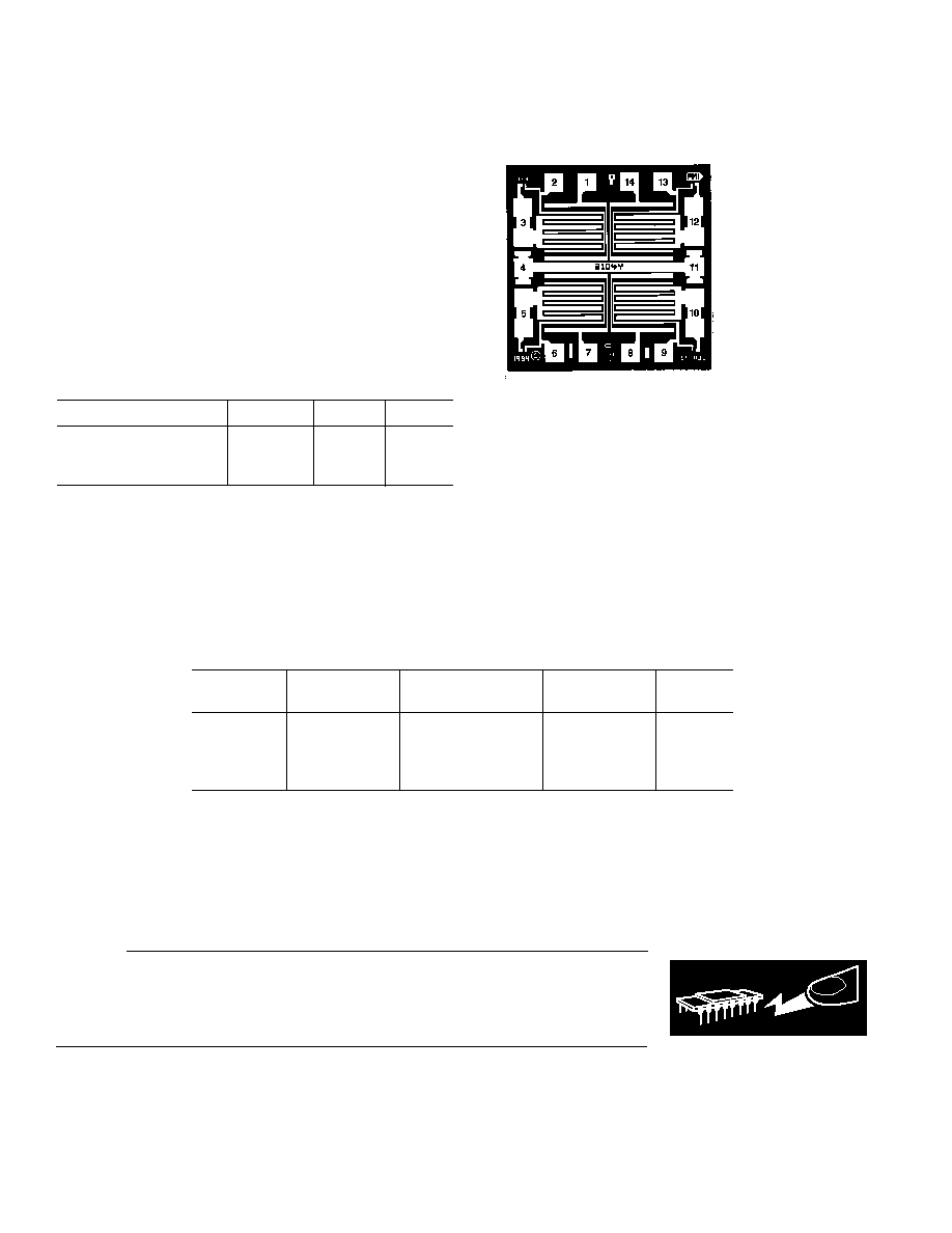
DICE CHARACTERISTICS
Die Size 0.060
◊ 0.060 Inch, 3600 Sq. mm
(1.52
◊ 1.52 mm, 2.31 sq. mm)
1.
Q1 COLLECTOR
2.
Q1 BASE
3.
Q1 EMITTER
4.
SUBSTRATE
5.
Q2 EMITTER
6.
Q2 BASE
7.
Q2 COLLECTOR
8.
Q3 COLLECTOR
9.
Q3 BASE
10. Q3 EMITTER
11. SUBSTRATE
12. Q4 EMITTER
13. Q4 BASE
14. Q4 COLLECTOR
MAT04
≠5≠
REV. D
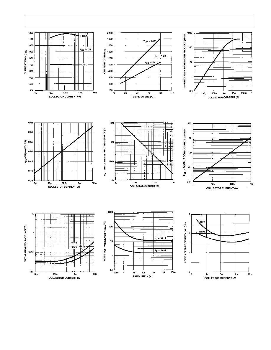
TPC 1. Current Gain
vs. Collector Current
TPC 4. Base-Emitter-On-Voltage
vs. Collector Current
TPC 7. Saturation Voltage vs.
Collector Current
TPC 2. Current Gain
vs. Temperature
TPC 5. Small Signal Input Resistance
(h
ie
) vs. Collector Current
TPC 8. Noise Voltage Density
vs. Frequency
TPC 3. Gain Bandwidth vs.
Collector Current
TPC 6. Small Signal Output
Conductance vs. Collector Current
TPC 9. Noise Voltage Density
vs. Collector Current
Typical Performance Characteristics≠
REV. D
MAT04
≠6≠
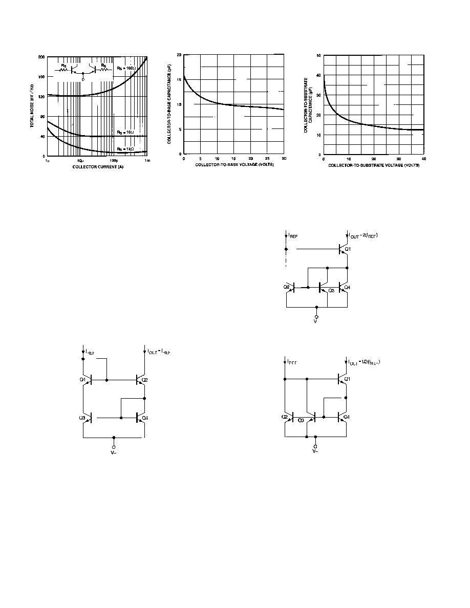
TPC 11. Collector-to-Base
Capacitance vs. Collector-to-
Base Voltage
TPC 12. Collector-to-Substrate
Capacitance vs. Collector-to-
Substrate Voltage
TPC 10. Total Noise vs.
Collector Current
APPLICATION NOTES
It is recommended that one of the substrate pins (Pins 4 and 11)
be tied to the most negative circuit potential to minimize cou-
pling between devices. Pins 4 and 11 are internally connected.
APPLICATIONS
CURRENT SOURCES
The MAT04 can be used to implement a variety of high imped-
ance current mirrors as shown in Figures 1, 2, and 3. These
current mirrors can be used as biasing elements and load de-
vices for amplifier stages.
Figure 1. Unity Gain Current Mirror, I
OUT
= I
REF
The unity-gain current mirror of Figure 1 has an accuracy of
better than 1% and an output impedance of over 100 M
at
100
ĶA. Figures 2 and 3 show modified current mirrors de-
signed for a current gain of two, and one-half respectively. The
accuracy of these mirrors is reduced from that of the unity-gain
source due to base current errors but is still better than 2%.
Figure 2. Current Mirror, I
OUT
= 2(l
REF
)
Figure 3. Current Mirror, I
OUT
= 1/2(I
REF
)
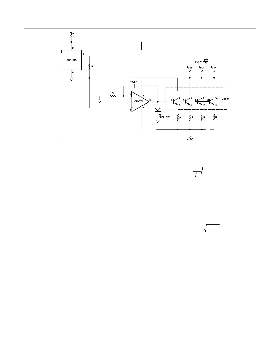
Figure 4 is a temperature independent current sink that has an
accuracy of better than 1% at an output current of 100
ĶA to 1
mA. The Schottky diode acts as a clamp to ensure correct cir-
cuit start-up at power on. The resistors used in this circuit
should be 1% metal-film type.
MAT04
≠7≠
REV. D
Figure 4. Temperature Independent Current Sink, I
OUT
= 10 V/R
NONLINEAR FUNCTIONS
An application where precision matched-transistors are a power-
ful tool is in the generation of nonlinear functions. These circuits
are based on the transistor's logarithmic property, which takes
the following idealized form:
V
kT
q
In
l
l
BE
C
S
=
The MAT04, with its excellent logarithmic conformance, main-
tains this idealized function over many decades of collector
current. This, in addition to the stringent parametric matching
of the MAT04, enables the implementation of extremely accu-
rate log/antilog circuits.
The circuit of Figure 5 is a vector summer that adds and sub-
tracts logged inputs to generate the following transfer function:
V
V
V
OUT
A
B
=
+
1
2
2
2
This circuit uses two MAT04 and maintains an accuracy of
better than 0.5% over an input range of 10 mV to 10 V. The
layout of the MAT04s reduces errors due to matching and
temperature differences between the two precision quad matched
transistors.
Op amps A1 and A2 translate the input voltages into logarithmic
valued currents (I
A
and I
B
in Figure 5) that flow through tran-
sistor Q3 and Q5. These currents are summed by transistor Q4
(
I
O
= I
A
+ I
B
=
l
l
1
2
2
2
+
),
which feeds the current-to-voltage converter consisting of op amp
A3. To maintain accuracy, 1% metal-film resistors should be used.
REV. D
MAT04
≠8≠
Figure 5. Vector Summer
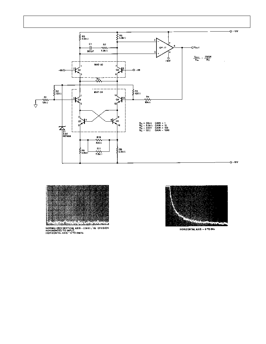
LOW NOISE, HIGH SPEED INSTRUMENTATION
AMPLIFIER
The circuit of Figure 6 is a very low noise, high speed amplifier,
ideal for use in precision transducer and professional audio
applications. The performance of the amplifier is summarized in
Table I. Figure 7 shows the input referred spot noise over the
0≠25 kHz bandwidth to be flat at 1.2 nV/
Hz. Figure 20 high-
lights the low 1/f noise corner at 2 Hz.
The circuit uses a high speed op amp, the OP17, preceded by
an input amplifier. This consists of a precision dual matched-
transistor, the MAT02, and a feedback V-to-I converter, the
MAT04. The arrangement of the MAT04 is known as a "linear-
ized cross quad" which performs the voltage-to-current conversion.
The OP17 acts as an overall nulling amplifier to complete the
feedback loop. Resistors R1, R2, and R3, R4 form voltage divid-
ers that attenuate the output voltage swing since the "cross
quad" arrangement has a limited input range. Biasing for the in-
put stage is set by Zener diode Z1. At low currents, the effective
zener voltage is about 3.3 V due to the soft knee characteristic of
the Zener diode. This results in a bias current of 530
ĶA per
side for the input stage. The gain of this amplifier with the val-
ues shown in Figure 6 is:
V
V
R
OUT
IN
G
=
33000
Table I. Instrumentation Amplifier Characteristics
Input Noise
G = 1000
1.2 nV/
Hz
Voltage Density
G = 100
3.6 nV/
Hz
G = 10
30 nV/
Hz
Bandwidth
G = 500
400 kHz
G = 100
1 MHz
G = 10
1.2 MHz
Slew Rate
40 V/
Ķs
Common-Mode Rejection G = 1000
130 dB
Distortion
G = 100
f = 20 Hz to 20 kHz
0.03%
Settling Time
G = 1000
10
Ķs
Power Consumption
350 mW
MAT04
≠9≠
REV. D
Figure 6. Low Noise, High-Speed Instrumentation Amplifier
Figure 7. Spot Noise of the Instrumentation Amplifier
from 0≠25 kHz, Gain Of 1000
Figure 8. Low Frequency Noise Spectrum Showing Low
2 Hz Noise Corner, Gain = 1000
REV. D
MAT04
≠10≠
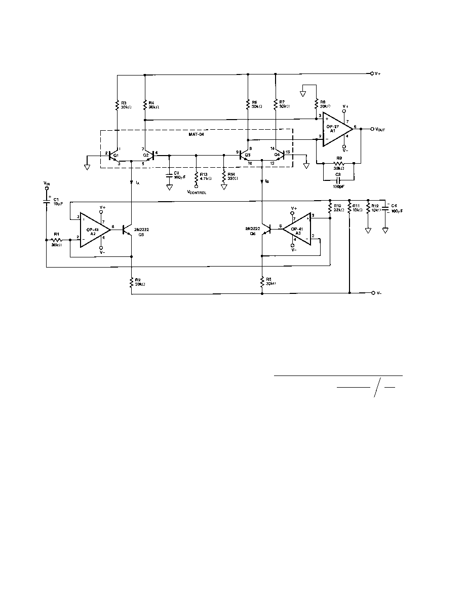
VOLTAGE-CONTROLLED ATTENUATOR
The voltage-controlled attenuator (VCA) of Figure 9, widely
used in professional audio circles, can easily be implemented
using a MAT04. The excellent matching characteristics of the
MAT04 enables the VCA to have a distortion level of under
0.03% over a wide range of control voltages. The VCA accepts a
3 V RMS input and easily handles the full 20 Hz≠20 kHz audio
bandwidth as shown in Figure 10. Noise level for the VCA is
more than 110 dB below maximum output.
In the voltage controlled attenuator, the input signal modulates
the stage current of each differential pair. Op amps A2 and A3
in conjunction with transistors Q5 and Q6 form voltage-to-current
converters that transform a single input voltage into differential
currents which form the stage currents of each differential pair.
The control voltage shifts the current between each side of the
two differential pairs, regulating the signal level reaching the
output stage which consists of op amp A1. Figure 11 shows the
increase in signal attenuation as the control voltage becomes
more negative.
The ideal transfer function for the voltage-controlled
attenuator is:
V
V
R
R
R
kT
q
OUT
IN
CONTROL
/
exp (
)
=
+
+
2
1
14
13
14
Where
k = Boltzman constant 1.38
◊ 10
≠23
J/
įK
T = temperature in
įK
q = electronic charge = 1.602
◊ 10
≠19
C
From the transfer function it can be seen that the maxi-
mum gain of the circuit is 2 (6 dB).
To ensure best performance, resistors R2 through R7 should
be 1% metal film resistors. Since capacitor C2 can see small
amounts of reverse bias when the control voltage is positive, it
may be prudent to use a nonpolarized tantalum capacitor.
Figure 9. Voltage-Controlled Attenuator
MAT04
≠11≠
REV. D
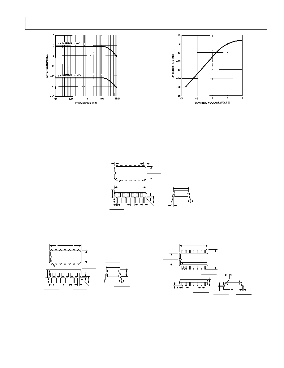
Figure 10. Voltage-Controlled Attenuator,
Attenuation vs. Frequency
Figure 11. Voltage-Controlled Attenuator,
Attenuation vs. Control Voltage
14-Lead Narrow-Body SO
(R-14/SO-14)
14
8
7
1
0.3444 (8.75)
0.3367 (8.55)
0.2440 (6.20)
0.2284 (5.80)
0.1574 (4.00)
0.1497 (3.80)
PIN 1
SEATING
PLANE
0.0098 (0.25)
0.0040 (0.10)
0.0192 (0.49)
0.0138 (0.35)
0.0688 (1.75)
0.0532 (1.35)
0.0500
(1.27)
BSC
0.0099 (0.25)
0.0075 (0.19)
0.0500 (1.27)
0.0160 (0.41)
8
į
0
į
0.0196 (0.50)
0.0099 (0.25)
x 45
į
14-Lead Plastic DIP
(N-14)
14
1
7
8
0.795 (20.19)
0.725 (18.42)
0.280 (7.11)
0.240 (6.10)
PIN 1
0.325 (8.25)
0.300 (7.62)
0.015 (0.381)
0.008 (0.204)
0.195 (4.95)
0.115 (2.93)
SEATING
PLANE
0.022 (0.558)
0.014 (0.356)
0.060 (1.52)
0.015 (0.38)
0.210 (5.33)
MAX
0.130
(3.30)
MIN
0.070 (1.77)
0.045 (1.15)
0.100
(2.54)
BSC
0.160 (4.06)
0.115 (2.93)
OUTLINE DIMENSIONS
Dimensions shown in inches and (mm).
14-Lead Cerdip
(Q-14)
14
1
7
8
0.310 (7.87)
0.220 (5.59)
PIN 1
0.005 (0.13) MIN
0.098 (2.49) MAX
SEATING
PLANE
0.023 (0.58)
0.014 (0.36)
0.200 (5.08)
MAX
0.785 (19.94) MAX
0.150
(3.81)
MIN
0.070 (1.78)
0.030 (0.76)
0.200 (5.08)
0.125 (3.18)
0.100
(2.54)
BSC
0.060 (1.52)
0.015 (0.38)
15
į
0
į
0.320 (8.13)
0.290 (7.37)
0.015 (0.38)
0.008 (0.20)

REV. D
MAT04
≠12≠
Revision History
Location
Page
Data Sheet changed from REV. C to REV. D.
Edits to ABSOLUTE MAXIMUM RATINGS . . . . . . . . . . . . . . . . . . . . . . . . . . . . . . . . . . . . . . . . . . . . . . . . . . . . . . . . . . . . . . . . . 1
Deleted ELECTRICAL CHARACTERISTICS for ≠55
įC . . . . . . . . . . . . . . . . . . . . . . . . . . . . . . . . . . . . . . . . . . . . . . . . . . . . . . . . 3
Deleted WAFER TEST LIMITS . . . . . . . . . . . . . . . . . . . . . . . . . . . . . . . . . . . . . . . . . . . . . . . . . . . . . . . . . . . . . . . . . . . . . . . . . . . 4
Edits to TPCs . . . . . . . . . . . . . . . . . . . . . . . . . . . . . . . . . . . . . . . . . . . . . . . . . . . . . . . . . . . . . . . . . . . . . . . . . . . . . . . . . . . . . . . . 5≠6
Added OUTLINE DIMENSIONS . . . . . . . . . . . . . . . . . . . . . . . . . . . . . . . . . . . . . . . . . . . . . . . . . . . . . . . . . . . . . . . . . . . . . . . . . 13
C00285-0-2/02(D)
PRINTED IN U.S.A.
Document Outline
- Specifications
- Pinout
- Package drawings
- Ordering Guide
- Features
- Product Description
- Absolute Maximum Ratings
- Typical Characteristics
- PRODUCT DESCRIPTION
- DICE CHARACTERISTICS
- APPLICATION NOTES
- APPLICATIONS
- CURRENT SOURCES
- NONLINEAR FUNCTIONS
- AMPLIFIER
- VOLTAGE-CONTROLLED ATTENUATOR
- Revision History
- Diagrams
- Unity Gain Current Mirror, IOUT = IREF
- Current Mirror, IOUT = 2(lREF)
- Current Mirror, IOUT = 1/2(IREF)
- Temperature Independent Current Sink, IOUT = 10 V/R.
- Vector Summer
- Low Noise, High-Speed Instrumentation Amplifier
- Voltage-Controlled Attenuator